- HOME
- TOP
- Products & Solutions
- Laser Processing Machines
- Laser Patterning
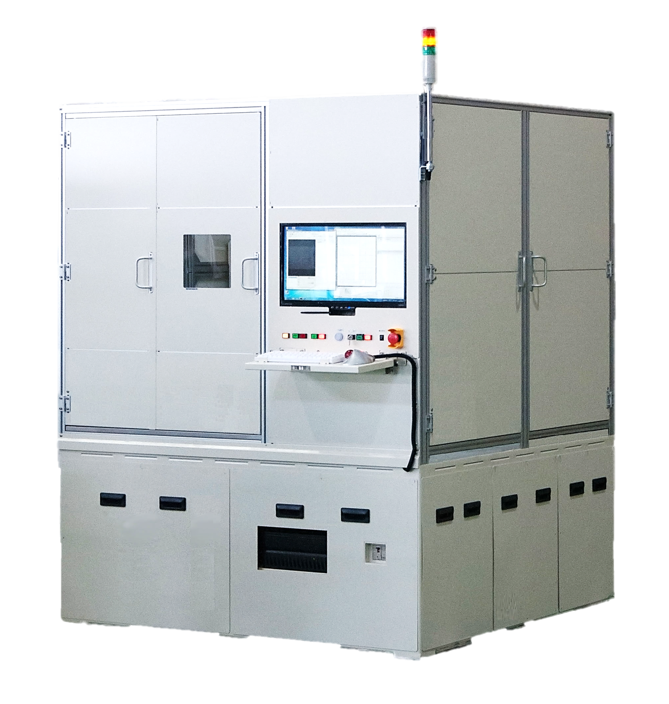
Laser Patterning Machine
A laser patterning machine is a dry processing system that uses laser light to form circuit and element patterns on functional thin films on glass substrates or film substrates. It eliminates the need for photomasks, allows for easy pattern changes, and reduces costs and environmental impact by eliminating the need for cleaning processes. A digital galvanometer scanner and high-precision stage enable uniform and fine patterning, making it suitable for applications such as fine line formation in ITO films and silver pastes, including displays, touch panels, semiconductors, and solar cells.
- A wide range of wavelengths can be selected.
- Uniform and high-precision machining
- High-speed and flexible machining
- Suitable for both mass-produced and prototype models.
Laser Patterning
The laser patterning process is a dry process that forms the patterns of circuits and elements required for each device. Laser selectively removes various types of functional laminated films formed on a glass substrate or film substrate.
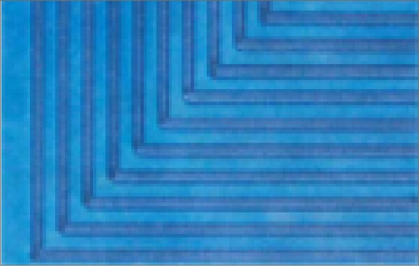
ITO film patterning on glass substrate
Line width: 25μm
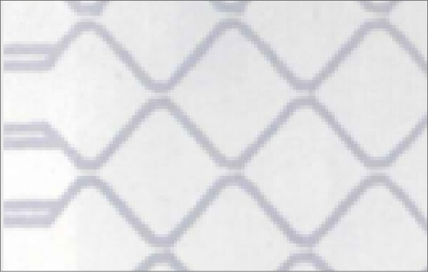
ITO film patterning on film
Line width:30μm
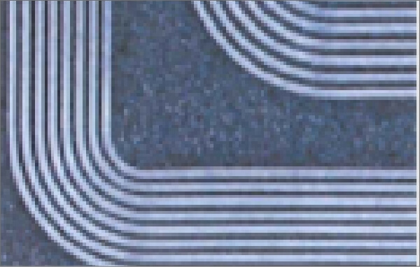
Silver paste patterning on film
Line width: 25μm
The system has been widely used for especially electrode formation of transparent films such as ITO, silver nanowire, CNT and silver paste.
Features of Laser Patterning
- ▶The laser light source can be selected from near-infrared wavelength to ultraviolet wavelength, so it can be used in various applications.
- ▶Flexible patterning with high-speed output control of laser light.
- ▶Steady laser scan speed enables a uniform processing.
- ▶High-accuracy patterning combined digital Galvano scanner and drive stage.
- ▶Offering 3types of systems ranging from R&D use to mass-produce use.
①Compared to photo-etching
- PC data, instead of using photomask, makes it easy to change and modify patterns.
- Fewer processes achieve man-hours and cost reduction. Maintenance cost for equipment investment also can be reduced.
- Running cost and environmental impact are reduced due to it being a dry process.
②Compared to screen printing
- Capable of <50μm microscopic pattern.
- No exposure mask
③Compared to ink-jet printing
- Compatible with materials that cannot be converted into ink.
- Forming thin-film pattern of <100nm is possible.
Contact us
Use Applications
Mobile/Touch Panel
- Laser patterning of transparent conductive film
- Laser patterning of extraction electrodes on touch screen
Organic Light Emitting Display (OLED)
- Laser patterning of transparent conductive film
- Trimming of function membrane
Automobile
- Laser patterning of transparent conductive film
- Laser patterning of extraction electrodes on touch screen
- Parts surface treatment/marking
Digital Appliance
- Fine hole drilling
- Marking
Semiconductor/Solar cell
- Scribing thin film
- Marking
Batch-type Laser Patterning Equipment
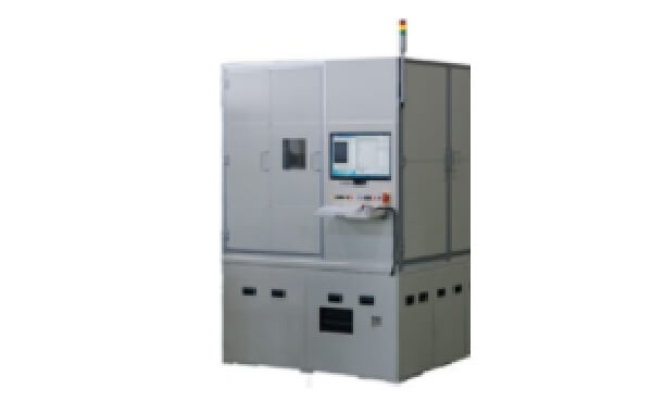
TLPS series
A batch-type patterning device equipped with a digital Galvano scanner and a high-precision workpiece positioning stage.
We can handle from production to prototyping in circuit formation for touch panel displays and organic EL devices.
Standard board dimension is 500×500, but we can design it according to your application and size.
Under the best conditions, microfabrication with a width of 10 μm is possible.
Laser Patterning Equipment for R&D and Preproduction
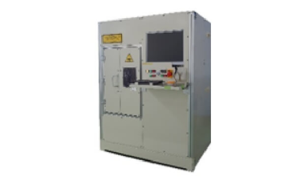
TLSM -202
Compact and low cost laser patterning system specialized for R&D and preproduction.
It can used for workpieces such as glass or film substrates.
Digital Galvano scanner enables advanced high-accuracy patterning, which is suitable for next-generation development. Standard board dimension is 500×500, but we can design it according to your application.
Roll-to-Roll Laser Patterning System
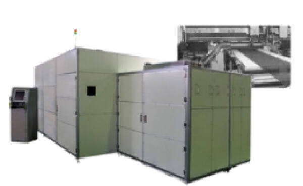
TLRP series
A laser patterning device for roll-shaped films and long workpieces.
Setting a workpiece on a reeler enables consecutive processing.
In order to realize high-precision and high-speed patterning, the standard mechanism combines a linear drive gantry stage and a digital Galvano scanner. We will select the optimum mechanism, and laser type and wavelength according to your request.